- Supply voltage range: 2-5.5V
- 16-bit ADC
- Continous current consumption: 150uA
- I2C interface
- Internal Oscillator
- Programmable data rate: 8SPS to 860SPS
- 860 samples/second over I2C
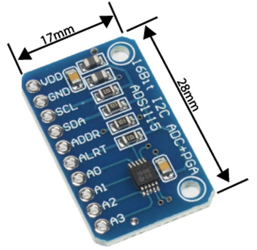
The ADS1115 module has 10 pins. The table below mentions all the pins on the module and the function of each pin type.
| Pin Type | Description |
| VDD | Voltage Input |
| GND | Ground |
| SCL | I2C Serial Clock |
| SDA | I2C Serial Data |
| ADDR | Address Pin |
| ALRT | Alert/Ready |
| A0 | Analog Input 1 |
| A1 | Analog Input 2 |
| A2 | Analog Input 3 |
| A3 | Analog Input 4 |
Why use an ADS1115 ADC Module
All the controllers have an ADC(analog-to-digital converters) as the microcontrollers only understand a digital signal. So to convert an incoming analog signal into a digital signal to be read by an MCU, an ADC is required. Now, the existing ADC’s in the microcontroller boards are not as precise and scalable as you would want them to be as the resolution of those ADC are not that good. Where modules like ADS1115 come into play.
An Arduino, for example, has a 10-bit ADC which can provide us an analog output from a range of 0 to 1023. Using a high-resolution ADC, like 16-bit ADS1115 opens up a scope to read out analog data with much higher precision and a scale of up to 65536(65000 approx). This means, even if the input signal is of a smaller level, it can be scaled onto this range and provide more precise and accurate results.
The module also has a PGA(Programmable Gain Amplifier) feature which allows us to multiply the very small analog signal values by a variable and obtain a higher signal value. For example, if a small signal of about 1mV is to be read, now if we use this feature we can multiply the input value of 1mV to a variable and obtain a higher value which can be precisely read as an output.
Functional Block Diagram of ADS1115 ADC
Below is the functional block diagram of an ADS1115.
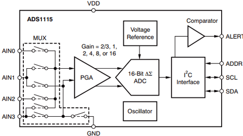
The analog inputs are passed on through a multiplexer which is then fed to the programmable gain amplifier, to amplify the input signal. The amplified signal is passed onto a 16-bit ADC whose output is provided to a microcontroller via I2C communication.
Interfacing ADS1115 Module with an MCU/MPU
Interfacing an ADS1115 ADC module to an MCU/MPU is easy. As discussed above, the ADC module communicates via I2C communication.
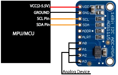
SCL(Serial Clock) and SDA(Serial Data) on the module are to be connected to the SCL and SDA pin on the MCU, respectively. 2 pins are for power; VDD and ground which can be connected to the 5V pin and ground of an MCU, respectively. A0, A1, A2, A3 are four analog input pins, which are to be connected to an analog source(potentiometer, etc).
ADS1X15 library for Arduino:
https://github.com/adafruit/Adafruit_ADS1X1
Applications of ADS1115
Here are some of the applications of ADS1115:
- Can be used as a Comparator
- Used for Battery monitoring systems
2D Model of ADS1115
Below is the 2 model of the ADS1115 ADC module along with its dimensions in millimeters. These dimensions can be used to create custom footprints of the module for PCB and CAD modeling.